Overview
A team of MIT physicists has used a one-molecule-thick material to demonstrate the thinnest LEDs and solar cells in the world. They apply an electric field onto an ultrathin sheet of their special material, thereby making it a semiconductor without adding any chemical “doping impurities”—the irreversible process often used by industry. In their process, by reversing the electric field the MIT researchers can turn the sheet into either of the two important semiconductor configurations—p-type or n-type. When they make one end of it p-type and the other end n-type, the sheet acts as a diode, the basic building block of electronics. Using their diodes, the physicists have built LEDs, solar cells, and light sensors that—once optimized by their engineering colleagues—could become ultrathin, lightweight, flexible devices suitable for mounting on buildings, weaving into clothing, and more.
Since graphene was isolated a decade ago, researchers worldwide have been using this one-atom-thick form of carbon for many potential applications, from faster computer chips to more efficient solar cells and desalination membranes. Four years ago, the research community was again invigorated when a whole family of materials was discovered that could be “exfoliated” in the same way that single sheets of graphene are lifted off chunks of graphite.
Pablo Jarillo-Herrero, the Mitsui Career Development Associate Professor of Physics, describes the phenomenon in terms of cards. A complete deck of cards is the standard “bulk” material. Take off one card and you have a single layer of the same material. “It turns out that the properties of an individual card are very different from the properties of the whole deck, and that’s what makes it surprising and fascinating,” he says.
For the past two years, Jarillo-Herrero and his team—Britton Baugher PhD ’14, graduate student Yafang Yang, and Hugh Churchill, Pappalardo Postdoctoral Fellow, all of the MIT Department of Physics—have been investigating one member of the family of materials, tungsten diselenide (WSe2). A single layer of WSe2 is actually three atoms thick: A layer of tungsten atoms at the center is enclosed by layers of selenium atoms above and below. “So the ‘monolayer’ is like a sandwich, but it’s still less than 1 nanometer thick,” says Jarillo-Herrero. “That’s about 50,000 times thinner than a human hair.”
Like graphene, single-layer WSe2 is semitransparent, flexible, strong, and—unlike bulk WSe2—it’s a good semiconductor. While it doesn’t naturally conduct electricity, getting current to flow requires adding just a few more carriers of electric charge, for example, electrons. Given its physical features and its properties, Jarillo-Herrero believes that single-layer WSe2 could one day make possible a host of new cheap, low-weight, flexible, semitransparent optical and electronic devices. He and his team are using a novel approach to help make that possible.
Making an electrically controlled p-n junction
In a pure semiconductor, electrons—negatively charged subatomic particles—are typically trapped within their atoms. Getting them to move along as current is usually achieved by adding a dopant—a few atoms of another chemical. The dopant may add free electrons to the material, giving it extra negative charge and making it an n-type material. Or the dopant may have electrons missing in its crystal structure—vacancies called holes, which effectively add extra positive charge and create a p-type material. As an electron moves from hole to hole, it creates a new hole in its former location, so in essence the negatively charged electrons move one way and the positively charged holes the other way through the material.
Making an electrically doped semiconductor
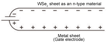
Figure 1. Producing a doped semiconductor generally involves introducing a few atoms of another material that add extra electrons or holes (vacancies where electrons are missing)—an irreversible process that permits current to flow. The MIT researchers have developed a novel, reversible way to achieve the same end in their three-atom-thick sheet of tungsten diselenide (WSe2). They place a sheet of metal beneath the WSe2 sheet, separated by an insulator (not shown above) and connected by a battery. Applying a voltage between the two sheets, which are in close proximity, induces an electric field, which causes electrons to flow to one sheet and holes to flow to the other. The orientation of the battery determines whether the WSe2 sheet becomes an n-type material (with extra electrons, shown here) or a p-type material (with extra holes).
The goal of doping semiconductors is, of course, to produce the extra electrons and holes. The chemical dopants are just carriers of those charged particles. But with ultrathin materials like WSe2, says Jarillo-Herrero, we don’t need the chemicals. Instead, he and his team employ a technique that adds electrons and holes to a sheet of WSe2 using only electric fields.
Figure 1 shows how it works. Take a sheet of WSe2 and place a thin sheet of metal under it. Separate them by an insulator and connect them at one end by a battery. (The essential geometry is that of a parallel plate capacitor, where one of the plates is the ultrathin WSe2.) If the bottom sheet—the “gate electrode”—is sufficiently close to the WSe2 sheet and a voltage is applied between the two sheets, an electric field is created. Holes move to one sheet, electrons to the other. The WSe2 sheet is now a doped semiconductor. Moreover, whether it’s p-type or n-type depends on which way around the battery is oriented. A negatively charged gate electrode will repel electrons away from the WSe2 sheet, thus leaving holes on it and making it a p-type semiconductor; a positively charged gate electrode will attract electrons to the WSe2, making it an n-type semiconductor. Thus, switching from one kind of semiconductor to the other requires simply turning the battery around.
Even more interesting, the researchers can make a sheet of WSe2 that’s half n-type and half p-type. As shown in Figure 2, two separate gate electrodes are connected by batteries to opposite ends of the WSe2 sheet. With the batteries in opposite directions, the gate electrodes will have opposite charge. As a result, one end of the WSe2 sheet will become p-type, the other end, n-type. The region of interest is where the p and n sections meet. Called the p-n junction, this interface is where much of the action takes place in semiconductor-based optoelectronic devices, that is, devices that manipulate interactions of light and electricity.
Creating a p-n junction
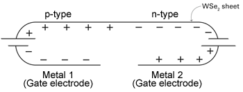
Figure 2. This setup makes half of the WSe2 sheet a p-type semiconductor and the other half an n-type. Two separate sheets of metal are connected by batteries to opposite ends of the WSe2 sheet. With the batteries in opposite directions, one end of the sheet receives extra electrons, the other end accumulates extra holes. Where the n-type section and p-type section of the WSe2 sheet meet is called a p-n junction—the interface at the core of most electronic devices.
A one-way valve for electricity
Having realized a p-n junction in their atomically thin material, the MIT team did what researchers have done with conventional p-n junctions for decades: They made a diode. A critical element in electrical circuits, the diode is essentially a switch that allows current to flow in one direction but not the other.
To demonstrate the behavior, the researchers connect an electrical circuit to the WSe2 p-n device, incorporating another battery to provide the “bias” voltage needed to make it operate. First they set it up with a positive bias voltage, which supplies negative electrons to the n-type end. Since electrons from the n-type end can move across the junction into holes in the p-type end, current flows through the circuit. They then turn the battery around to send current in the opposite direction through the circuit. Now the negative bias voltage sends electrons into the p-type end, but electrons can’t move across the junction into the n-type end, so no current flows.
Figure 3 shows results of experiments using the WSe2 diode set up as a p-n junction. When the bias voltage is negative, there’s little or no flow of current. When the bias voltage switches to positive, current begins to flow and soon jumps up by a hundred thousand times. When the p and n ends of the WSe plate are swapped, the shape of the curve showing current flow is almost a mirror image of the one shown in the diagram. The electrically induced p-n and n-p junctions thus act as successful—and flexible—diodes.
According to Jarillo-Herrero, the new diodes have properties that are very close to “ideal,” as defined in textbooks. Indeed, they are far closer to the textbook definition of ideal than are diodes made of organic semiconductors—materials now being pursued because they are cheap, flexible, semitransparent, and can be grown over large areas. “Our new diodes aren’t meant to compete with traditional semiconductor diodes of silicon or gallium arsenide,” says Jarillo-Herrero. “We see them more as possible alternatives to organic electronics, which have many of the same attractive physical characteristics.”
Tests of the WSe2-based diode
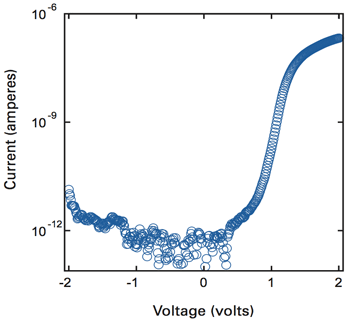
Figure 3. This figure shows the flow of current through the WSe2 p-n diode as voltage varies. When voltage is negative, little or no current flows. Changing to positive voltage brings a sudden increase in current. The WSe2 diode is thus effective as a switch that permits current to flow one way but not the other.
Jarillo-Herrero stresses the adaptability of their WSe2 diodes. “Usually when you make a diode, the p-type and n-type ends are fixed by the chemical impurities that you’ve added. You can’t change a p-n diode to an n-p diode,” he says. “We have three batteries— three voltages—that allow us to control the whole thing. We can do anything we want because we electrically tune it with a knob.”
Beyond diodes
Given their novel high-performance diodes, the next step was to build optoelectronic devices. There are three basic devices that one can make with a diode: a photovoltaic solar cell, a light-emitting diode (LED), and a photodetector (a light sensor). “We realized for the first time in an atomically thin material all three of those functionalities,” says Jarillo-Herrero.
All of their devices work well. For example, their photovoltaic cell converts incoming photons (packets of solar energy) into flowing electrons with notable efficiency, given the small amount of material available for absorbing incoming sunlight. Their LED emits visible light that’s focused in a relatively narrow wavelength range—a property that generally correlates to brightness. As shown in Figure 4, WSe2 emits red light most strongly. But other members of the same chemical family emit other colors, so in principle several could be combined to produce various colors and mixtures. Finally, the response of their photodetector matches that of conventional commercial sensors that are much bigger and bulkier.
Demonstration of the WSe2-based LED
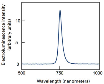
Figure 4. This curve shows the intensity of light emitted at various wavelengths by the WSe2 p-n LED when current passes through it. Intensity peaks at about 750 nm—the red part of the visible spectrum.
The semiconductor at the core of each of those devices is just three atoms thick. But what about other components? With the exception of the batteries, they could all be made of ultrathin materials, says Jarillo-Herrero. The gate electrodes and the contacts with the batteries could be made of one-atom-thick graphene, and the insulator between the gates and the WSe2 sheet could be a single nanometer of hexagonal boron nitride. Jarillo-Herrero and his team are beginning to develop some of those components now.
Future plans
In principle, the novel WSe2-based devices could one day lead to a new class of commercial electronic and optoelectronic products. Industrial processes exist for making very large-area sheets of WSe2; and while selenium is far more rare than, say, silicon, the amount of WSe2 used in the atomically thin devices is so small that thousands of times less material would be needed to make devices of a given size.
Jarillo-Herrero stresses that “it’s still early on, and a lot of research has to be done.” Thus far, he and his team have made only proof-of-concept devices. Even so, they were surprised at how well their devices performed in this first trial. “We’re physicists, not engineers, so we don’t iterate and optimize things,” he says. “But I think it’s fair to say that already these devices are surprisingly good—and that’s why the engineers are jumping on it.”
At the invitation of Marc A. Baldo, professor of electrical engineering, and Vladimir Bulović, the Fariborz Maseeh Professor of Emerging Technology and associate dean for innovation in MIT’s School of Engineering, Jarillo-Herrero and his group have joined the Center for Excitonics, an Energy Frontier Research Center directed by Baldo and supported by the US Department of Energy. Together, the physicists and engineers will investigate these new materials and their atomic properties in greater depth, and they’ll optimize the devices to improve their performance and move them toward efficient, inexpensive commercial products that can harvest, emit, and detect light.
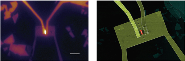
Above left: This image, taken through an optical microscope, shows the team’s experimental WSe2 LED. Electricity flows through platinum and gold wires (coming down from the top left and right) to the LED at the center, causing it to glow. The scale bar equals 5 micrometers. Image courtesy of Britton Baugher and Hugh Churchill. Above right: A scanning electron microscope image of the device. The glow at the LED center has been added for illustration purposes. Image: Felice Frankel and Jarillo-Herrero group.
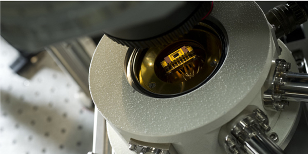
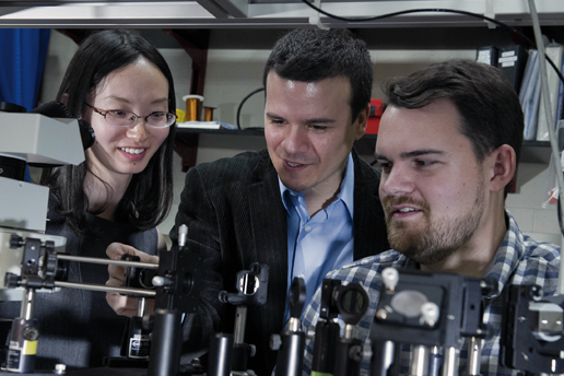
The researchers use this specially designed optical cryostat setup to examine and test their devices. Photo: Stuart Darsch
This research was supported by the US Office of Naval Research, a Packard fellowship, and a Pappalardo fellowship. It made use of National Science Foundation-supported facilities. Further information can be found in:
B.W.H. Baugher, H.O.H. Churchill, Y. Yang, and P. Jarillo-Herrero. “Optoelectronic devices based on electrically tunable p-n diodes in a monolayer dichalcogenide.” Nature Nanotechnology, vol. 9, April 2014, pp. 262–267.
B.W.H. Baugher. Electronic Transport in Atomically Thin Layered Materials. PhD thesis, MIT Department of Physics, May 2014.
This article appears in the Autumn 2014 issue of Energy Futures.