By combining expertise in electrical engineering, nanotechnology, and quantum chemistry, MIT researchers are making novel solar cells that could one day be twice as efficient as current cells are. Their design calls for multiple layers of nanoscale materials that are tuned to capture more of the energy in sunlight and meshed to minimize energy loss within the cell. The layers can be deposited on silicon wafers or plain glass using inexpensive room-temperature processes such as ink-jet printing or silk screening.
These devices are ideally suited for investigating exactly what physical processes contribute to overall performance, with the goal of achieving higher efficiencies. “With the devices we’re building we expect to be able to dissect every process we observe cleanly enough to explore one phenomenon at a time and consequently get clear answers on how to optimize performance,” says Vladimir Bulović, associate professor of electrical engineering and co-director of the Eni-MIT Solar Frontiers Center.

Professor Vladimir Bulović, co-director of the Eni-MIT Solar Frontiers Center, and his collaborators are working on novel solar cells that could one day be twice as efficient as current cells are. Photo: Greg Hren Photography/Research Laboratory of Electronics at MIT
If photovoltaic (PV) solar power is to compete economically with conventional power sources, PV modules and system installation must become significantly less expensive—a change that can be accomplished by increasing PV power conversion efficiencies and by scaling up the production of PV modules. Bulović suggests that both of those goals can be achieved by using large-area printed thin films of nanoscale materials—tiny chunks of matter measured in billionths of a meter. “We can use thin films of molecules, polymers, or quantum dots,” Bulović says. “Such nanoscale forms of matter can be optimally designed to absorb light and generate photoaction.”
The challenge is to identify the most appropriate nanostructured materials for PV applications and then to control their precise assembly at the nanoscale while depositing them over the large areas needed for PV modules.
Choosing the right materials
The first step in understanding the benefits of nanostructures is to understand how PV systems work. When photons strike a material, electrons absorb energy and jump from their low-energy “ground” state to their high-energy “excited” state. That process leaves vacancies—called holes—where electrons are missing. The electrons and holes remain loosely bound. In a solar cell, the trick is to separate them so the electrons can flow through an external circuit.
That separation is generally achieved by using a second type of material whose energy level is lower. Arriving at the interface between the materials, the electrons see an opportunity to lose some of their extra energy, so they move into the second material. Over time, holes accumulate in the first material and electrons in the second. Connect the outside edges of the two materials by a loop of wire and the electrons will flow back to the first material, powering a light bulb or other device along the way.
Bulović cites two approaches to material selection that can help optimize the process just described. One key is choosing the correct difference, or “offset,” between the energy levels of the electrons in the two materials. The energy dissipated when an excited electron jumps from one material to the other should be just enough to cause the electron to make the move. Any extra dissipation reduces the energy available for powering the light bulb. So fine-tuning the energy offset at the interface between the two materials is one means of increasing efficiency.
Another means is to choose the correct “band gap” for each material, that is, the difference in energy between the electrons’ ground and excited states. The band gap determines what color light, or wavelength, the material will absorb and emit. Silicon PV cells—the most widely deployed PV technology—have a band gap that is nearly ideally tuned to maximize the conversion efficiency of the sun’s light energy to electrical power, yielding PV modules that are 8 to 14 percent efficient. Because they are optimized to respond to the sun’s broad visible light spectrum, silicon PVs do not do well with ultraviolet light or infrared light. (The former is strongly absorbed but also strongly reflected by the silicon PV surface, while much of the latter simply passes through.) A silicon solar cell combined with additional PV cells made from materials that can absorb those poorly utilized wavelengths should capture and convert more of the energy in sunlight.
“The first step in making a good solar cell is to get the right spacing between energy levels within the individual materials and the right positions with respect to the neighbor’s energy levels,” explains Bulović.
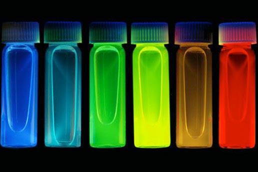
Finding materials that have exactly the right energy levels would be difficult. Bulović therefore turns to his colleague Moungi G. Bawendi, Lester Wolfe Professor in Chemistry and an expert in creating nanomaterials with specially tuned band gaps and energy levels. Bawendi’s specialty is the quantum dot, a tiny chunk of material that is just a dozen or so atoms across. In a particle of that size, electrons are unable to move around as much as they’d like to. Because the electrons are confined, they become more energetic. Indeed, the energy levels and band gap are determined by the exact size of the particle. “So with a quantum dot, you can fine-tune its band gap over a very broad range simply by varying the size of the material,” says Bulović. And Bawendi is a master at it. “You can name the color you would like to absorb, and his group can make nano-crystals that are precisely tuned to absorb it,” Bulović notes.
Depositing the nano layers
The researchers’ next job is to deposit those quantum dots—or polymers, organic molecules, metal oxides, or other nanoscale materials—so that they work together to capture as much of the solar spectrum as possible and to separate the photogenerated electrons and holes efficiently. Bulović is not the first to make such combinations. Others have made blended structures in which the different materials are mixed together. But with many blended structures, it is hard to know exactly what physical processes are controlling the performance of the device. Bulović likens the approach to putting salad in a bowl and mixing it all up. “It is easy—and technologically very attractive—to make simple PV devices by mixing two nanoscale materials into a photoactive emulsion, spreading it as a thin film, and then laminating contacts on the top,” he explains. “It is, however, challenging to understand how things work inside such devices and what steps to take to improve their performance.”
Instead, Bulović, Bawendi, and their colleagues are creating layered structures with distinctly defined interfaces that will allow them to probe and optimize the operating mechanisms of nano-PVs. “We’re perfecting the interfaces by making layered-cake-type structures, where you have a layer that does one thing, another layer that does something else, and so on,” says Bulović. “Through the careful chemical design of band gaps and interface offsets we can learn about the governing processes in these nanostructured PVs.”
Bulović has extensive experience with creating stacked structures of multiple materials. For over a decade, he and his colleagues have been developing multilayered molecular thin films to demonstrate organic LEDs that can be used as paper-thin TV screens and similarly slim photodetector planes of nanoscale thickness. Extending this molecular work to colloidal quantum dots, Bulović and Bawendi recently developed new printing techniques that can deposit thin layers of quantum dots on top of a substrate of choice—just the type of process they now need in their development of nano-PVs.
Using their novel printing methods, the researchers have created stacked nanostructured PVs. They can layer the nanomaterials on flexible substrates such as rollable plastic or metal foils, or they can deposit them on conventional silicon-based PVs to form “tandem” structures with boosted efficiency. Because of the crystalline nature of silicon, meshing it with other crystalline semiconductors is not easy. Nanomaterials, on the other hand, work fine because they are created in an optically active form before being deposited on the silicon. As a result, the researchers can use simple room-temperature processes, such as printing of nanostructured inks, stamping, or silk screening.
Conversion targets
According to Bulović, first-principles calculations suggest that if they do everything exactly right using a single nanostructured layer on top of silicon, they should achieve 15 percent efficient conversion—somewhat better than today’s commercial PVs. But if they combine multiple layers that are good at absorbing differing parts of the spectrum, theory says that they should get up to 25 percent power conversion.
Thus far, the efficiencies of their devices are far from that high, but Bulović sees no reason that they cannot get there. “The goal is achievable,” he says. “We just need to understand the detailed physical phenomena that govern the operation of these nanostructured photovoltaics.” And their layered structures are an ideal “bench top” on which to explore those physical processes and identify the exact parameters that yield the best operation.
This nanoscale photovoltaic research is part of the research agenda of the Eni-MIT Solar Frontiers Center. The initial part of the research program was supported by the MIT Institute for Soldier Nanotechnologies, a grant from the U.S. Army Research Office, and the Presidential Early Career Award for Scientists and Engineers, which was awarded to Bulović by the White House in 2004. Also, this work made use of the MRSEC Shared Experimental Facilities at MIT, supported by the National Science Foundation. Further information can be found in www.mtl.mit.edu/research/annual_reports/2007/pdf/mn/mn3_17.pdf.
This article appears in the Autumn 2008 issue of Energy Futures.