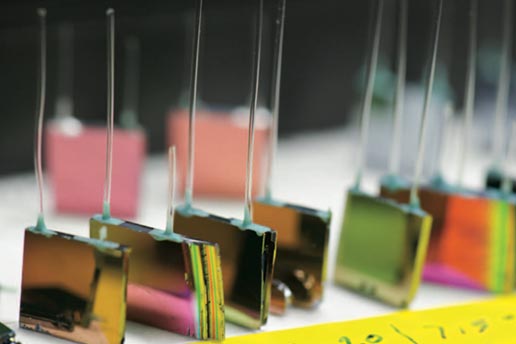
A novel MIT technology is now making possible remarkably efficient photovoltaic (PV) systems that can be powered by the sun, a hydrocarbon fuel, a decaying radioisotope, or any other source of heat. The key to the efficient operation: a specially engineered material that absorbs the heat and then—because of billions of nanoscale pits on its surface—selectively radiates to the PV cell only those wavelengths that the cell can convert into electricity.
Based on that technology, the MIT researchers have fabricated a button-sized power generator that’s fueled by butane, can run three times longer than a lithium-ion battery of the same weight, and can be recharged instantly by snapping in a tiny cartridge of fresh fuel. Another device, powered by a radioisotope, should generate electricity for 30 years without refueling or servicing—an ideal source of electricity for spacecraft that head out of our solar system.
According to the US Energy Information Administration, 92% of all the energy we use involves converting heat into mechanical energy and then often into electricity. But today’s mechanical systems have drawbacks: their reliability is poor (moving parts can break); their efficiency is relatively low; and they can’t be successfully scaled down to the small sizes needed to match so many of today’s power-consuming devices, from sensors to smart phones to medical monitors.
“Being able to convert heat from various sources into electricity without moving parts would bring huge benefits,” says Ivan Celanovic ScD ’06, research engineer in the Institute for Soldier Nanotechnologies (ISN), “especially if we could do it efficiently, relatively inexpensively, and on a small scale—a few millimeters, centimeters, or meters.”
PV cells are solid-state electricity generators—and they needn’t always run on sunlight. Half a century ago, researchers developed thermophotovoltaics (TPV), an approach that couples a PV diode (the active part of a solar cell) with any source of heat. In a TPV system, a burning hydrocarbon, for example, heats up a solid piece of material called the thermal emitter; the thermal emitter radiates heat and light onto the PV diode; and the PV diode generates electricity. Because the thermal emitter is not as hot as the sun is, its radiation includes far more infrared wavelengths than occur in the solar spectrum. “Low band-gap” PV materials invented less than a decade ago can absorb more of that infrared radiation than standard silicon PVs can; but much of the heat is still wasted, so efficiencies remain relatively low.
An ideal match
The solution, says Celanovic, is to design a thermal emitter that radiates only the wavelengths that the PV diode can absorb and convert into electricity—and suppresses emission of all other wavelengths. “If you have perfect spectral matching between your heat source and your PV diode, you’ll get optimal efficiency for the overall system,” he says.
“But how do we find a material that has this magical property of emitting only at the wavelengths that we want?” asks Marin Soljačić, associate professor of physics and ISN researcher. The answer: make a photonic crystal. Take a sample of material and on its surface create some nanoscale features—say, a regularly repeating pattern of holes or ridges. Light will now propagate through the sample in a dramatically different way than it did when the material was in its natural form.
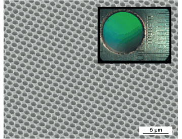
Using new nanofabrication techniques, MIT researchers made these samples of tungsten with billions of regularly spaced, uniform nanoscale holes on their surfaces. In their TVP system, this type of photonic crystal serves as a thermal emitter, absorbing heat and then—because of its surface structure—radiating to the PV diode only those wavelengths that the diode can convert into electricity. The inset shows a digital photo of the full 1 cm-diameter sample, illuminated by white light. The color suggests the diffraction of white light into green as a result of the surface pattern.
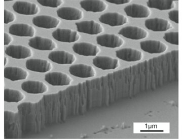
“By choosing how we design the nanostructure, we can create materials that have novel optical properties,” says Soljačić. “This gives us the ability to control and manipulate the behavior of light.”
This powerful approach—co-developed by John D. Joannopoulos, the Francis Wright Davis Professor of Physics and ISN director, and others—has been widely used to improve lasers, light- emitting diodes, and even optical fibers. But to the MIT team, this new type of material was exactly what they needed to engineer the spectrum of their thermal radiation to what their PV diode could use.
Designing the photonic crystal
To start, they needed a material that could be heated to extremely high temperatures and then glow with an intensely bright light. The obvious choice was tungsten, which for 100 years has served as the filament in incandescent light bulbs. To make a slab of tungsten into a photonic crystal, they created an array of tiny pits—cylindrical cavities—on the surface. When the slab heats up, it generates a bright light but now with an altered emission spectrum.
Why? Each pit acts as a resonator, capable of giving off radiative heat at only certain wavelengths. It thus provides wavelength selectivity. Celanovic offers as an analogy an acoustic resonator. “It’s kind of like when you put a seashell next to your ear and you hear a humming noise. You hear the noise amplified at the resonant frequencies of the seashell cavity. It’s the same principle, the same physics, but rather than acoustic resonance, this is electromagnetic resonance,” he says.
To implement their “designer material,” the researchers needed to find a practical means of fabricating a nanoscale structure in tungsten. After much work, they developed a method based on lithography and reactive ion etching, processing techniques used to make small features, for example, on micro-processors. In their case, interference between two overlapping laser beams creates an etch mask with identical tiny holes, which are then transferred to a tungsten substrate by reactive ion etching. Using that approach, the MIT team has fabricated tungsten photonic crystals that are 1 cm in diameter with surfaces that contain billions of tiny holes, equally spaced from one another and nearly uniform in diameter and depth.
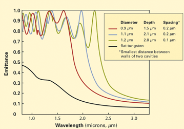
This diagram demonstrates how manipulating the nanostructure of the tungsten photonic crystal can affect the spectrum of the light it emits. (Emittance is an indicator of radiation efficiency.) In this example, the three colored spectra come from heated tungsten samples that contain nanoscale holes of differing diameters, depths, and spacing. Those differing geometries dramatically change the dominant wavelengths in the emitted light. The spectrum drawn in black is from a sample of tungsten with a smooth surface.
The diagram above demonstrates how manipulating the surface geometry changes the spectral emittance of a photonic crystal. The curves show thermal emittance at various wavelengths. The spectrum drawn in black is from a heated tungsten sample that has a smooth surface. The three colored spectra are from tungsten samples that contain holes of differing diameters, depths, and spacing. As a result, their emission spectra are distinctly different. “So by changing the geometrical parameters of a photonic crystal for a given material, you can tune the cutoff between where it radiates and where it doesn’t radiate,” says Celanovic.
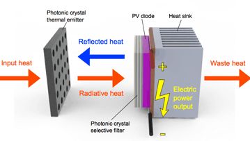
In this novel MIT design, input heat from an energy source raises the temperature of the tungsten photonic crystal, which transmits radiative heat at selected wavelengths to the PV diode. A second photonic crystal—mounted on the face of the PV diode—lets through heat at wave- lengths that the diode can convert into electricity and reflects the rest back to the tungsten photonic crystal, where it is reabsorbed and reemitted. Electricity from the PV diode passes to an electronic circuit that adjusts its voltage to match the external device being powered.
The diagram above shows the basic setup of their photonic crystal-enabled TPV system. Heat from a source at the left raises the temperature of the tungsten photonic crystal—the thermal emitter—which radiates heat at selected wavelengths toward the PV diode, and the diode converts it into electric power. Despite careful tailoring, the tungsten emitter delivers some heat at wavelengths that the PV diode cannot convert into electricity. To prevent that waste, the researchers mount on the face of the diode another photonic crystal, this one fabricated with a series of alternating layers of silicon and silicon dioxide—a nanostructure that can be tailored to transmit certain wavelengths and reflect others. Here, it reflects any radiation at unacceptable wavelengths back to the tungsten emitter, where it is reabsorbed and subsequently reemitted to provide more heat at wavelengths that the PV diode can use.
Deploying their novel TPV system
Using this TPV system, the MIT team is working with collaborators at MIT and elsewhere to create several novel electricity-generating devices. One example is the micro-TPV power generator, a button-sized solid-state device that uses as its heat source hydrocarbon fuels such as butane or propane. At the heart of the device is a “micro-reactor” designed by Klavs Jensen, the Warren K. Lewis Professor of Chemical Engineering, and fabricated in the Microsystems Technology Laboratories. This tiny reactor is a silicon chip with an interior channel where injected fuel undergoes catalytic reaction, generating heat. Photonic crystals are deposited on the top and bottom surfaces of the micro-reactor, and low band-gap PV diodes are placed above and below the reactor separated by tiny gaps. Heated by the micro-reactor, the TPV system generates electricity, which passes to an electronic circuit that was specially designed by Robert Pilawa, graduate student, and David Perreault, associate professor, both of electrical engineering and computer science. The circuit dynami-cally adjusts the voltages and currents to suit a smart phone, sensor, or other device while extracting the maximum amount of power from the TPV system.
Each of these silicon chips is a micro-reactor with photonic crystals on both faces and external tubes for injecting fuel and air and ejecting waste products. Inside an interior channel, the fuel and air react, heating up the photonic crystals. In a complete system, that heat would pass to electricity-generating PV diodes that would be mounted just above and below each face, separated by a tiny gap. Photos: Justin Knight
Prototypes of their micro-TPV power generator are “pretty exciting,” says Celanovic. The devices achieve a fuel-to-electricity conversion efficiency of about 3%—a ratio that may not sound impressive, but at that efficiency their energy output is three times greater than that of a lithium ion battery of the same size and weight. The TPV power generator can thus run three times longer without recharging, and then recharging is instantaneous: just snap in a new cartridge of butane. With further work on packaging and system design, Celanovic is confident that they can triple their current energy density. “At that point, our TPV generator could power your smart phone for a whole week without being recharged,” he says.
Other work focuses on using radioisotopes—materials that undergo radioactive decay, giving off heat in the process. Their energy density can be orders of magnitude higher than that of chemical fuels, and radioisotopes need not be dangerous. (Indeed, some are used in pacemakers that are implanted for 10 years.) A TPV power generator fueled by a radioisotope could run for three or more decades and could be ideal for certain high-level applications that need electricity for years but are difficult or impossible to access for recharging. In one project, for example, the MIT team is working with collaborators at NASA and Creare, Inc. (Hanover, NH) to develop a radioisotope-based TPV generator for deep space probes—a setting where even the best rechargeable batteries and solar panels are not an option.
Finally, the researchers are looking at ways to use their photonic crystal to improve the conversion of solar energy into electricity. For example, optical concentrators such as parabolic mirrors could focus solar radiation onto a photonic crystal absorber and emitter, which would reshape the solar spectrum to better match the properties of a PV cell. Collaborators are members of the Solid State Solar Thermal Energy Conversion Center, which is directed by Gang Chen, the Carl Richard Soderberg Professor of Power Engineering.
Celanovic and Soljačić stress that building practical systems requires integrating many technologies and fields of expertise. “It’s a really multidisciplinary effort,” says Celanovic. “And it’s a neat example of how fundamental research in materials can result in new performance that enables a whole spectrum of applications for efficient energy conversion.”
This research was supported in part by a seed grant from the MIT Energy Initiative. Research on the micro-TPV system was supported in part by the US Army Research Office through the Institute for Soldier Nanotechnologies. The radioisotope-TPV work was supported in part by the NASA Glenn Research Center under the Small Business Technology Transfer Program. The Solid State Solar Thermal Energy Conversion Center is supported by the US Department of Energy. Further information can be found in:
P. Bermel, M. Ghebrebrhan, W. Chan, Y. Yeng, M. Araghchini, R. Hamam, C. Marton, K. Jensen, M. Soljačić, J. Joannopoulos, S. Johnson, and I. Celanovic. “Design and global optimization of high-efficiency thermo- photovoltaic systems.” Optics Express 18, pp. A314-A334, 2010.
I. Celanovic, N. Jovanovic, and J. Kassakian. “Two-dimensional tungsten photonic crystals as selective thermal emitters.” Applied Physics Letters, v. 92, 193101, 2008.
M. Ghebrebrhan, Y. Yeng, P. Bermel, I. Celanovic, M. Soljačić, and J. Joannopoulos. “Tailoring thermal radiation from metallic photonic crystal slabs via coupled-mode theory.” Physical Review A, v. 83, 033810, 2011.
R. Pilawa-Podgurski, N. Pallo, W. Chan, D. Perreault, and I. Celanovic. “Low-power maximum power point tracker with digital control for thermophotovoltaic generators.” Proceedings of the Twenty-Fifth Annual IEEE Applied Power Electronics Conference, APEC 2010, pp. 961–967, February 2010.
This article appears in the Spring 2011 issue of Energy Futures.