MIT researchers have designed a new transistor that could significantly reduce wasted electricity whenever voltage must be modified, for example, when recharging a laptop or hooking solar panels into the power grid. Widespread use of the novel transistor could cut US electricity consumption as well as give new life to emerging energy technologies ranging from electric cars and solar cells to revolutionary power generation and transmission systems.
Power electronics are used to change the form of electrical energy to match a given need. In particular, many new electronic devices and energy technologies require switching alternating current (AC) to direct current (DC) or vice versa. For example, batteries and solar cells deal only in DC. Therefore, recharging a laptop or cell phone battery requires changing the AC electricity coming from the wall outlet to DC. Conversely, connecting solar cells to the power grid and running the motor in an electric car both require converting DC to AC. At a larger scale, high-voltage DC transmission lines can transfer large amounts of power with lower electrical losses than AC lines can, but their use is now limited because converting DC to AC is expensive.
“Power electronics are used in many different places in our lives,” says Tomás Palacios, assistant professor of electrical engineering and computer science. “But any time you transform electricity, there are always energy losses—and with today’s devices, those losses are high.” If we could reduce the losses in all power electronic circuits, Palacios says, we could save between 10 percent and 20 percent of the total electricity now used in the United States. And if we could make the power electronics small, we could integrate them into the equipment that needs them. Small, efficient power electronics that could switch AC to DC and back again would be a game-changer for electric cars, power grids, renewable energy technologies—indeed, for the world’s ability to meet the overall energy challenge.
To help improve power electronics, Palacios and graduate student Bin Lu of electrical engineering and computer science are working on one of the key components—the transistor. This basic building block can serve as either a switch or an amplifier; it can turn on and off or increase or decrease the current flowing in an electronic circuit.
A transistor consists of several layers of semiconductor linked to the circuit by three terminals. The electrons that carry the electric current enter the transistor through the first terminal (called the source). They then travel through a region of the semiconductor called the channel and exit via the second terminal (the drain). A small electrical charge on the third terminal (the gate) influences the channel’s ability to conduct electricity. A transistor thus uses a small charge to regulate the flow of a large current.
How well the transistor performs depends in large part on two properties of the semiconductor. First, it must have low resistance so electrons can flow through it with ease. Any impediment to that flow produces heat, which translates into wasted electricity. Second, the semiconductor must be able to handle high voltages without “breaking down,” that is, without allowing the current to jump from the source to the drain as a spark. If the breakdown voltage of the semiconductor is high, the source and drain can be located close to one another without sparking; as a result, the transistor can be smaller, which permits the overall power circuit to be smaller and more efficient.
According to Palacios, the desired properties can be found in a family of compounds and alloys based on nitride semiconductors. Gallium nitride (GaN), for example, is a relatively new semiconductor that has a resistance 100 to 1,000 times lower than the best semiconductors now being used commercially. In addition, its breakdown voltage can be 10 times higher than in conventional devices.
However, despite their promise, GaN-based transistors for power electronics are not yet commercially available. Palacios cites three problems with the designs now being considered. First, the best devices to date are grown on a substrate of silicon carbide, an extremely expensive material. Second, in those devices, electrons can escape from the channel via the gate terminal, thereby being lost from the circuit. And finally, if there is no charge on the gate, electrons continue to flow through the transistor. That characteristic—known as being “normally on”—is a safety hazard. If, for example, the gate stops functioning while a laptop is recharging, household current could flow at full voltage into the computer and quickly destroy it.
The MIT design
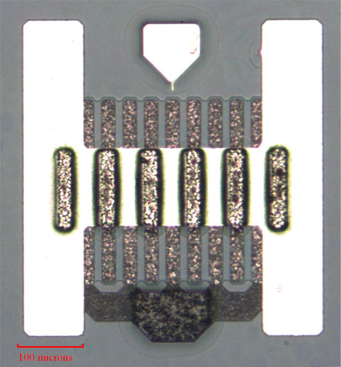
Top-view optical micrograph of one of the gallium nitride power transistors fabricated at MIT. Photo: Daniel Piedra G, MIT
Palacios and his team therefore set three goals for their GaN transistor: to use a less expensive substrate, to keep resistance low while preventing electrons from escaping via the gate, and to make a device that is “normally off.” They have now achieved all of those goals.
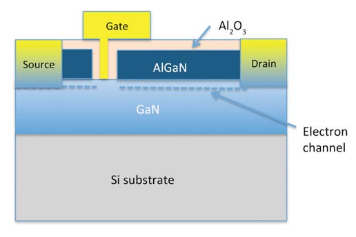
Their design is shown in the diagram in the right-hand column. Electrons—indicated by blue dashes—enter through the source at the upper left, pass through the GaN semiconductor, and exit through the drain at the upper right. The amount of charge on the gate at the top regulates the flow of electrons from the source to the drain.
Specific features address the researchers’ three goals. To bring down costs, they build their transistor on a silicon substrate similar to that used by much of today’s electronics industry. It is inexpensive and can be manufactured using standard technology for making commercial silicon chips.
To lower the resistance in the GaN channel, the researchers put a layer of aluminum gallium nitride (AlGaN) on top of the GaN. That layer produces a high density of electrons in the GaN just below the GaN/AlGaN interface, easing the flow of current through the channel and reducing the total resistance of the device. “The electrons really like to move through the GaN very close to that interface,” says Palacios. In addition, to prevent electrons from going into the gate contact, they add a thin layer of a dielectric—aluminum oxide (Al2O3), a highly insulating material that completely stops the flow of electrons to the gate.
Finally, they have developed a new fabrication technology—called “dual-gate technology”—to make the transistor normally off. Traditional approaches to achieving normally off transistors involve thinning down the AlGaN layer under the gate. That change reduces the electron density in the GaN channel to the point that electrons will not flow in the absence of charge on the gate. However, that approach introduces very high resistance, which leads to heating and thus energy losses in the device.
To overcome this problem, the MIT researchers make the gate “T” shaped and then omit the AlGaN layer completely from a very narrow region beneath the foot of the T. Because no AlGaN is deposited in that region, no electrons are left near the interface; and when there is no charge on the gate, current no longer flows. But the removed section of AlGaN is less than 100 nm—just wide enough to create the normally off conditions but still so narrow that it does not significantly increase the resistance of the transistor. And because the thin layer of Al2O3 insulator separates the gate from the channel in that region, when electrons do flow, they cannot escape to the gate.
Fabricating prototypes
Palacios and his team have now successfully achieved each step needed to fabricate their novel transistor. They have developed methods of using thin layers of GaN on silicon wafers, of depositing the Al2O3 insulator, and of fabricating normally off transistors using the new dual-gate technology. Tests of initial prototypes confirm that their device is normally off and that electrons are effectively confined to the channel near the GaN-AlGaN interface. “In fact, our preliminary measurements show that the electrons move along that channel 10 times faster than they do in other power devices,” says Palacios.
Encouraged by results to date, Palacios is already in discussion with other MIT researchers who might benefit from the small, efficient power electronics made possible by the new GaN transistor. Among the possibilities: new circuit designs for high-efficiency inverters and converters for the power industry, power modules for hybrid-vehicle and fuel-cell technologies, and—because of their tolerance for high temperatures—high-performance power electronics for new solar concentrators.
“With our new devices we should be able to maximize and optimize power conversion and add more intelligence to current and new power systems at a wide range of voltage levels,” says Palacios. “Transistors and power systems are ubiquitous, so the potential for saving energy and developing and implementing new energy technologies is substantial.”
This research was funded by a seed grant from the MIT Energy Initiative and by the US Department of Energy. Further information can be found in:
B. Lu and T. Palacios. “New enhancement-mode GaN HEMT based on dipole-engineering.” IEEE Electron Device Letters, forthcoming 2010.
B. Lu, E. Piner, and T. Palacios. High-Performance Dual-Gate AlGaN/GaN Enhancement-Mode Transistor. Presented at the 37th International Symposium on Compound Semiconductors (ISCS), Kagawa, Japan, May 31–June 4, 2010.
This article appears in the Spring 2010 issue of Energy Futures.