Sheets of graphene and other materials that are virtually two-dimensional hold great promise for electronic, optical, and other high-tech applications. But the biggest limitation in unleashing this potential has been figuring out how to make these materials in the form of anything larger than tiny flakes. Now researchers at MIT and elsewhere may have found a way to do so.
The group has determined a way to make large sheets of one such material, called molybdenum telluride, or MoTe2. The team says their method is also likely to work for many similar 2-D materials, and could make widespread applications feasible.
The findings have been published in the Journal of the American Chemical Society by a team including MIT postdoc Lin Zhou; professors Mildred Dresselhaus, Jing Kong, and Tomás Palacios; and eight others at MIT, the China University of Petroleum, Central South University in China, the National Tsing-hua University in Taiwan, and Saitama University and Tohoku University in Japan.
“This material has a similar bandgap to silicon” — a characteristic needed in order to make transistors and solar cells — “and in single-layer form it has a direct bandgap,” Zhou says, which allows better light emission. “It also has strong absorption for solar radiation,” which is key to making practical solar cells, she says.
Molybdenum telluride can exist in two different forms; one is metallic, meaning it conducts electricity well, and the other is a natural semiconductor, lending itself to applications in electronics. Controlling how the material is made allows the researchers to create whichever form is needed for a particular use.
The new method is based on chemical vapor deposition (CVD), and makes it possible to create sheets of any thickness, and of a size limited only by the dimensions of the CVD chamber used for deposition.
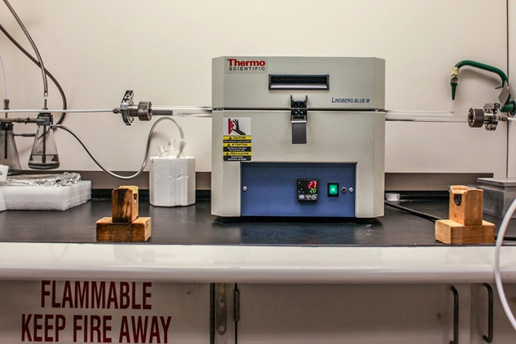
The chemical vapor deposition system for MoTe2 growth. Photo: Jose-Luis Olivares/MIT
One challenge the team had to overcome was that the atoms of molybdenum telluride are very weakly bound to each other, so the tendency of the two precursor materials to form molybdenum telluride is low. “This makes it more challenging to make, compared to other similar materials,” Zhou says.
The researchers were able to overcome this by using several stages of deposition, beginning with a layer of pure molybdenum. “This method makes it easy, because you only need to control one material,” Zhou says. This step is followed by oxidation of that layer; this material is then removed and powdered tellurium is added, vaporized in a carrier gas of hydrogen and argon, at a temperature of 700 degrees Celsius. The use of hydrogen in the process, the team found, is crucial to producing a uniform MoTe2 film.
The material should be immediately usable to create electronic devices including field-effect transistors, which the team has already demonstrated in the lab.
“Our process can grow sheets that have a very large area, are very homogeneous, and have high quality,” Zhou says.
The team now aims to explore adapting this process to create large sheets of other promising thin materials: “2-D materials are a big family with different properties,” Zhou says. She and her colleagues will examine whether versions of the process can work with other compounds.
Molybdenum telluride also lends itself to applications in spintronics, Zhou says, an emerging technology based on the spins of electrons rather than their charge, as in conventional electronics.
Physicist Ado Jorio of the Federal University of Minas Gerais, Brazil, who was not involved in this work, says, “What is most impressive is that this group has been able to consecutively develop new formulae to produce almost any low-dimensional material they want, always scalable with the highest quality worldwide.”
And Vincent Meunier, a physicist at Rensselaer Polytechnic Institute who was also not associated in this research, adds, “One of the many advantages of the proposed approach stems from its simplicity. The consequences of this development are likely to be numerous, as it provides a versatile and scalable technique to develop macroscopic amounts of atomically thin films, thereby surmounting major roadblocks faced by layered-materials based research so far.”
The work was supported by the National Science Foundation, the Office of Naval Research, and the International Postdoctoral Exchange Fellowship Program.