
In Brief
For quantum dot (QD) materials to perform well in devices such as solar cells, the nanoscale crystals in them need to pack together tightly so that electrons can hop easily from one dot to the next and flow out as current. MIT researchers have now made QD films in which the dots vary by just one atom in diameter and are organized into solid lattices with unprecedented order. Subsequent processing pulls the QDs in the film closer together, further easing the electrons’ pathway. Tests using an ultrafast laser confirm that the energy levels of vacancies in adjacent QDs are so similar that hopping electrons don’t get stuck in low-energy dots along the way. Taken together, the results suggest a new direction for ongoing efforts to develop these promising materials for high performance in electronic and optical devices.
In recent decades, much research attention has focused on electronic materials made of quantum dots (QDs), tiny crystals of semiconducting materials a few nanometers in diameter. After three decades of research, QDs are now being used in TV displays where they emit bright light in vivid colors that can be fine-tuned by changing the sizes of the nanoparticles.
But many opportunities remain for taking advantage of these remarkable materials. “QDs are a really promising underlying materials technology for energy applications,” says William Tisdale, ARCO Career Development Professor in Energy Studies and associate professor of chemical engineering. QD materials pique his interest for several reasons. QDs are easily synthesized in a solvent at low temperatures using standard procedures. The QD-bearing solvent can then be deposited on a surface—small or large, rigid or flexible—and as it dries, the QDs are left behind as a solid. Best of all, the electronic and optical properties of that solid can be controlled by “tuning” the QDs. “With QDs, you have all these degrees of freedom,” says Tisdale. “You can change their composition, size, shape, and surface chemistry to fabricate a material that’s tailored for your application.”
The ability to adjust electron behavior to suit specific devices is of particular interest. For example, in solar photovoltaics (PVs), electrons should pick up energy from sunlight and then move rapidly through the material and out as current before they lose their excess energy. In light-emitting diodes (LEDs), high-energy “excited” electrons should relax on cue, emitting their extra energy as light.
With thermoelectric (TE) devices, QD materials could be a game-changer. When TE materials are hotter on one side than the other, they generate electricity. So TE devices could turn waste heat in car engines, industrial equipment, and other sources into power—without combustion or moving parts. The TE effect has been known for a century, but devices using TE materials have remained inefficient. The problem: While those materials conduct electricity well, they also conduct heat well, so the temperatures of the two ends of a device quickly equalize. In most materials, measures to decrease heat flow also decrease electron flow. “With QDs, we can control those two properties separately,” says Tisdale. “So we can simultaneously engineer our material so it’s good at transferring electrical charge but bad at transporting heat.”
Making good arrays
One challenge in working with QDs has been to make particles that are all the same size and shape. During QD synthesis, quadrillions of nanocrystals are deposited onto a surface, where they self-assemble in an orderly fashion as they dry. If the individual QDs aren’t all exactly the same, they can’t pack together tightly, and electrons won’t move easily from one nanocrystal to the next.
Three years ago, a team in Tisdale’s lab led by Mark Weidman PhD ’16 demonstrated a way to reduce that structural disorder. In a series of experiments with lead-sulfide QDs, team members found that carefully selecting the ratio between the lead and sulfur in the starting materials would produce QDs of uniform size. “And as those nanocrystals dry, they self-assemble into a beautifully ordered arrangement we call a superlattice,” says Tisdale.
The figure below shows scattering electron microscope images of those superlattices taken from several angles. Images a and b are taken from the top and show lined-up, 5 nanometer (nm)-diameter nanocrystals on the surface. Images c and d show edges of superlattices and display the depth and long-range ordering of the QDs.
For a closer examination of their materials, Weidman performed a series of X-ray scattering experiments at the National Synchrotron Light Source at Brookhaven National Laboratory. Data from those experiments showed both how the QDs are positioned relative to one another and how they’re oriented, that is, whether they’re all facing the same way.
The results confirmed that QDs in the superlattices are well ordered and essentially all the same. “On average, the difference in diameter between one nanocrystal and another was less than the size of one more atom added to the surface,” says Tisdale. “So these QDs have unprecedented monodispersity, and they exhibit structural behavior that we hadn’t seen previously because no one could make QDs this monodisperse.”
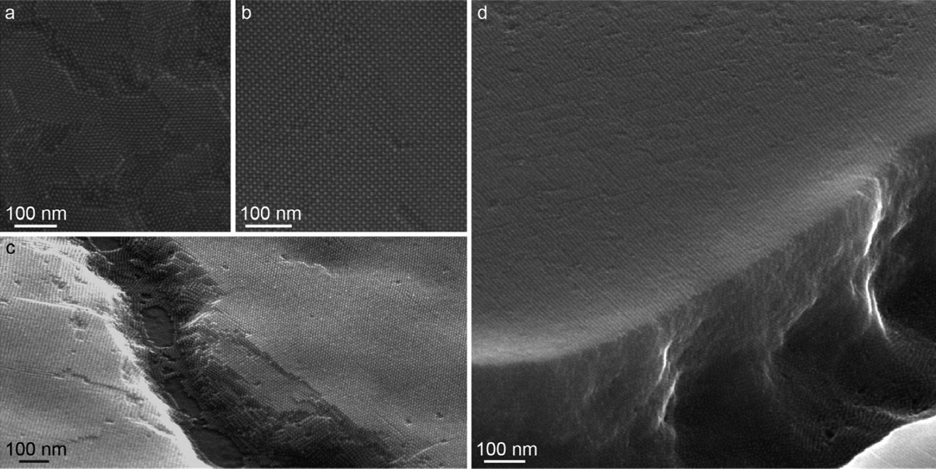
Micrographs of lead-sulfide quantum dot (QD) materials These images show scanning electron micrographs of sample QD films. The dark spots are the individual quantum dots, each about 5 nanometers (nm) in diameter. Images a and b show the consistent size and alignment of the QDs at the surface. The exposed edges in images c and d show depth and long-range ordering of the nanocrystals.
Controlling electron hopping
The researchers next focused on how to tailor their monodisperse QD materials for efficient transfer of electrical current. “In a PV or TE device made of QDs, the electrons need to be able to hop effortlessly from one dot to the next and then do that many thousands of times as they make their way to the metal electrode,” explains Tisdale.
One way to influence hopping is by controlling the spacing from one QD to the next. As shown in the schematics below, a single QD consists of a core of semiconducting material—in this work, lead sulfide—with chemically bound arms, or “ligands,” made of organic (carbon-containing) molecules radiating outward. The ligands play a critical role: Without them, as the QDs form in solution, they’d stick together and drop out as a solid clump. Once the QD layer is dry, the ligands end up as solid spacers that determine how far apart the nanocrystals are.
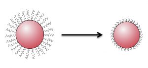
Structure of a quantum dot As shown these schematics, at the center of a quantum dot (QD) is a core of a semiconducting material. Radiating outward from that core are arms, or ligands, of an organic material. The ligands keep the QDs in solution from sticking together, and they determine the spacing between the dots in the solid product. Replacing the long ligands on the left with the short ones on the right allows the QDs to pack more closely together.
A standard ligand material used in QD synthesis is oleic acid. Given the length of an oleic acid ligand, the QDs in the dry superlattice end up about 2.6 nm apart—and that’s a problem. “That may sound like a small distance, but it’s not,” says Tisdale. “It’s way too big for a hopping electron to get across.”
Using shorter ligands in the starting solution—like those in the schematic above—would reduce that distance, but they wouldn’t keep the QDs from sticking together when they’re in solution. “So we needed to swap out the long oleic acid ligands in our solid materials for something shorter” after the film formed, says Tisdale.
To achieve that replacement, the researchers use a process called ligand exchange. First, they prepare a mixture of a shorter ligand and an organic solvent that will dissolve oleic acid but not the lead sulfide QDs. They then submerge the QD film in that mixture for 24 hours. During that time, the oleic acid ligands dissolve, and the new, shorter ligands take their place, pulling the QDs closer together. The solvent and oleic acid are then rinsed off.
Tests with various ligands confirmed their impact on interparticle spacing. Depending on the length of the selected ligand, the researchers could reduce that spacing from the original 2.6 nm with oleic acid all the way down to 0.4 nm. However, while the resulting films have beautifully ordered regions—perfect for fundamental studies—inserting the shorter ligands tends to generate cracks as the overall volume of the QD sample shrinks.
Energetic alignment of nanocrystals
One result of that work came as a surprise: Ligands known to yield high performance in lead-sulfide-based solar cells didn’t produce the shortest interparticle spacing in their tests. “Reducing that spacing to get good conductivity is necessary,” says Tisdale. “But there may be other aspects of our QD material that we need to optimize to facilitate electron transfer.”
One possibility is a mismatch between the energy levels of the electrons in adjacent QDs. In any material, electrons exist at only two energy levels—a low “ground state” and a high “excited state.” If an electron in a QD film receives extra energy—say, from incoming sunlight—it can jump up to its excited state and move through the material until it finds a low-energy opening left behind by another traveling electron. It then drops down to its ground state, releasing its excess energy as heat or light.
In solid crystals, those two energy levels are a fixed characteristic of the material itself. But in QDs, they vary with particle size. Make a QD smaller, and the energy level of its excited electrons increases. Again, variability in QD size can create problems. Once excited, a high-energy electron in a small QD will hop from dot to dot—until it comes to a large, low-energy QD. “Excited electrons like going downhill more than they like going uphill, so they tend to hang out on the low-energy dots,” says Tisdale. “If there’s then a high-energy dot in the way, it takes them a long time to get past that bottleneck.” So the greater mismatch between energy levels—called energetic disorder—the worse the electron mobility.
To measure the impact of energetic disorder on electron flow in their samples, Rachel Gilmore PhD ’17 and her collaborators used a technique called pump-probe spectroscopy—as far as they know, the first time this method has been used to study electron hopping in QDs.
QDs in an excited state absorb light differently than do those in the ground state, so shining light through a material and taking an absorption spectrum provides a measure of the electronic states in it. But in QD materials, electron hopping events can occur within picoseconds—10-12 of a second—which is faster than any electrical detector can measure.
The researchers therefore set up a special experiment using an ultrafast laser, whose beam is made up of quick pulses occurring at 100,000 per second. Their setup subdivides the laser beam such that a single pulse is split into a “pump” pulse that excites a sample and—after a delay measured in femtoseconds (10-15 seconds)—a corresponding “probe” pulse that measures the sample’s energy state after the delay. By gradually increasing the delay between the pump and probe pulses, they gather absorption spectra that show how much electron transfer has occurred and how quickly the excited electrons drop back to their ground state.
Sample results appear below. The top figure shows data from a QD sample with standard dot-to-dot variability. The bottom figure shows results from one of the monodisperse samples. In each case, the dotted lines indicate the starting and ending energy. In the sample with high variability, the excited electrons lose much of their excess energy within 3 nanoseconds. In the monodisperse sample, little energy is lost in the same time period—an indication that the energy levels of the QDs are all about the same.
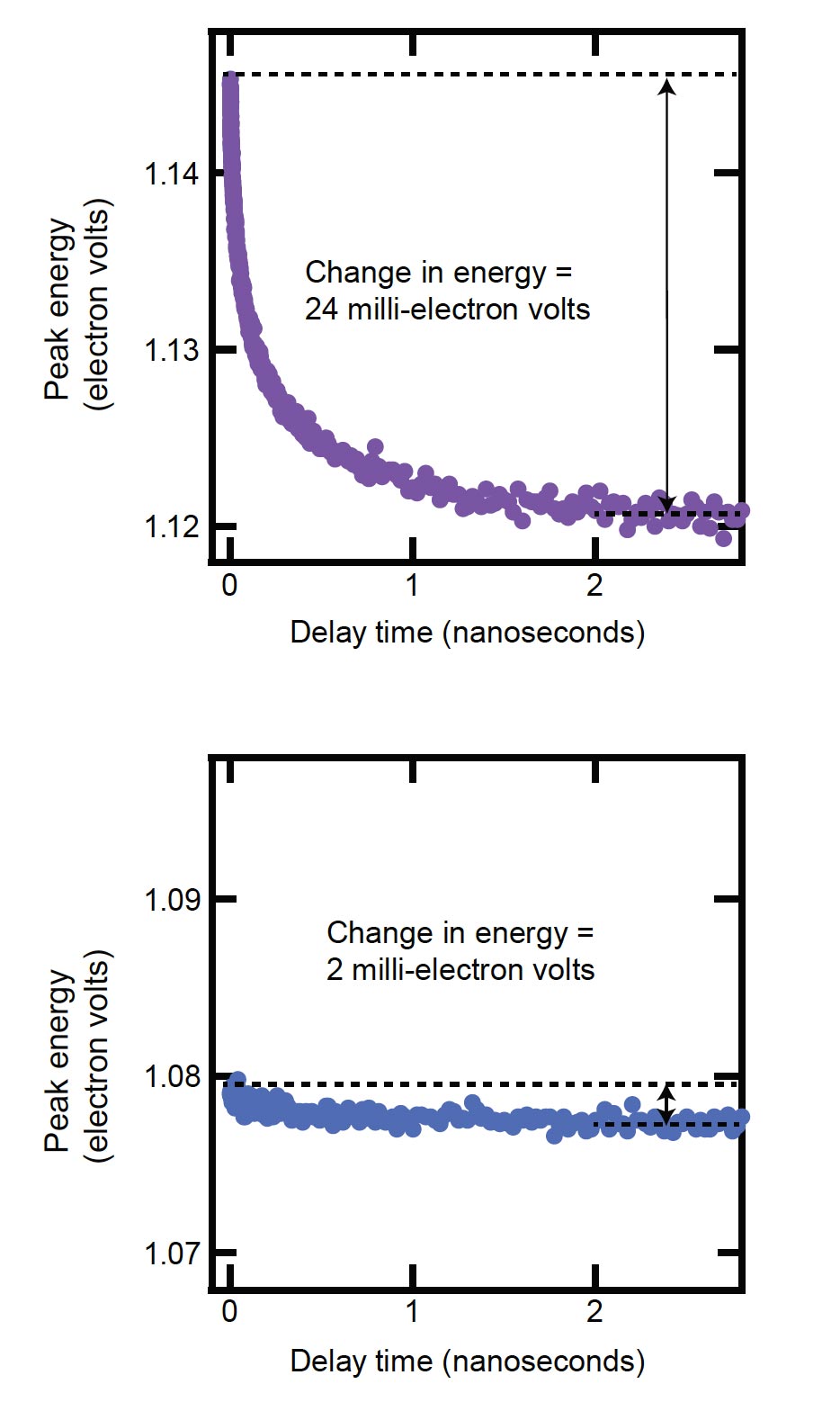
Results from ultrafast laser experiments These graphs show electron energy measurements in a standard QD film (top) and in a film made from monodisperse QDs (bottom). In each graph, the data points show energy measurements at initial excitation—indicated by the top dotted line—and over the subsequent 3 nanoseconds. In the standard sample, the electrons rapidly lose their excess energy. In contrast, in the monodisperse sample, the energy level remains fairly constant—an indication that the energy levels of the QDs are essentially uniform.
By combining their spectroscopy results with computer simulations of the electron transport process, the researchers extracted electron hopping times ranging from 80 picoseconds for their smallest quantum dots to over 1 nanosecond for the largest ones. And they concluded that their QD materials are at the theoretical limit of how little energetic disorder is possible. Indeed, any difference in energy between neighboring QDs isn’t a problem. At room temperature, energy levels are always vibrating a bit, and those fluctuations are larger than the small differences from one QD to the next. “So at some instant, random kicks in energy from the environment will cause the energy levels of the QDs to line up, and the electron will do a quick hop,” says Tisdale.
The way forward
With energetic disorder no longer a concern, Tisdale concludes that further progress in making commercially viable QD materials will require better ways of dealing with structural disorder. He and his team tested several methods of performing ligand exchange in solid samples, and none produced films with consistent QD size and spacing over large areas without cracks. As a result, he now believes that efforts to optimize that process “may not take us where we need to go.”
What’s needed instead is a way to put short ligands on the QDs when they’re in solution and then let them self-assemble into the desired structure. “There are some emerging strategies for solution-phase ligand exchange,” he says. “If they’re successfully developed and combined with monodisperse QDs, we should be able to produce beautifully ordered, large-area structures well suited for devices such as solar cells, LEDs, and thermoelectric systems.”
Critical to the ultrafast laser tests is the ability to create pump and probe pulses by subdividing a single pulse of laser light and creating a delay between when the two parts reach the sample. To achieve that effect, the researchers mount a partially reflective mirror on a motorized, moveable stage. They send part of the laser beam straight through the sample and divert the other part so that it passes through the sample after a fixed time delay measured in femtoseconds (10-15 seconds). The spectrum taken at a given pump pulse measures light absorption of electrons in their excited state; the spectrum at the corresponding probe pulse shows their energy state after the delay. By adjusting the location of the mirror and thus the time delay, the researchers can determine how much electron transfer has occurred as well as how quickly the excited electrons drop back to their ground state.
Notes
QD synthesis and spectroscopy were supported by the US Department of Energy, Office of Basic Energy Sciences. Structural studies of QD solids were supported by the MIT Energy Initiative Seed Fund Program. Mark Weidman and Rachel Gilmore were partially supported by a National Science Foundation Graduate Research Fellowship. Measurements were performed at the Center for Functional Nanomaterials at Brookhaven National Laboratory, the Cornell High Energy Synchrotron Source, and the MRSEC Shared Experimental Facilities at MIT. Further information can be found in:
R. Gilmore, E. Lee, M. Weidman, A. Willard, and W. Tisdale. “Charge carrier hopping dynamics in homogeneously broadened PbS quantum dot solids.” Nano Letters, vol. 17, pp. 893–901, 2017.
M. Weidman, M. Beck, R. Hoffman, F. Prins, and W. Tisdale. “Monodisperse, air-stable PbS nanocrystals via precursor stoichiometry control.” ACS Nano, vol. 8, no. 6, pp. 6363–6371, 2014.
M. Weidman, K. Yager, and W. Tisdale. “Interparticle spacing and structural ordering in superlattice PbS nanocrystal solids undergoing ligand exchange.” Chemistry of Materials, vol. 27, pp. 474–482, 2015.
This article appears in the Autumn 2017 issue of Energy Futures.